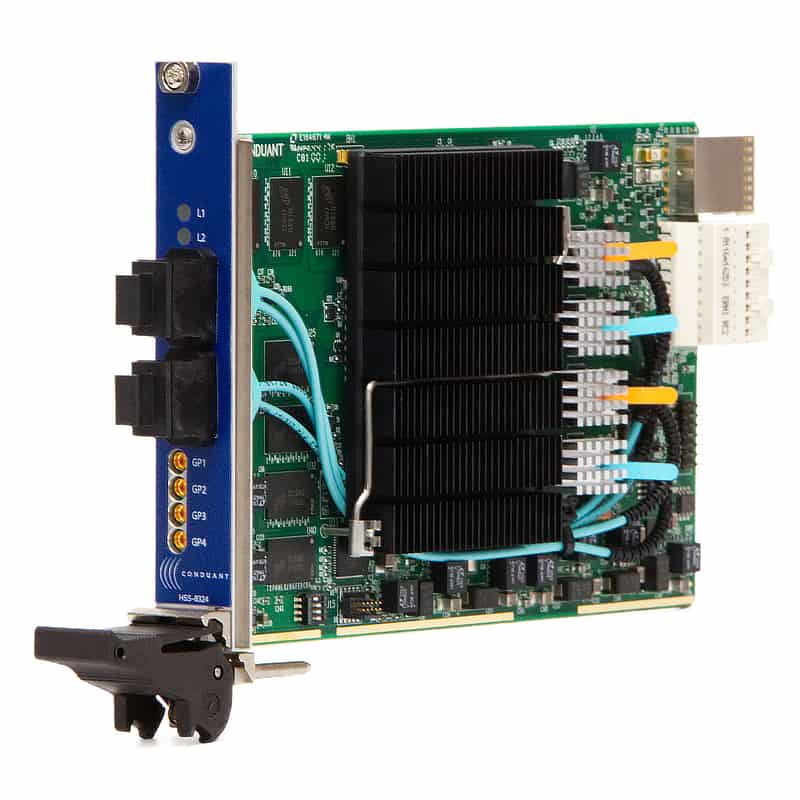
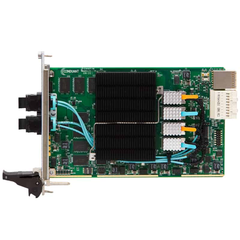
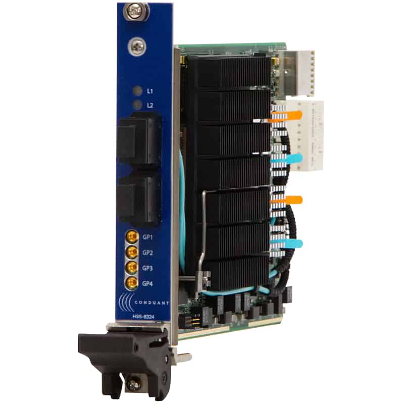
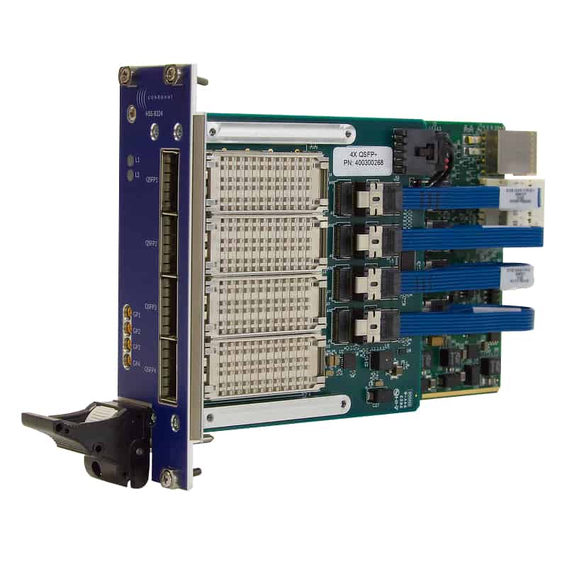
The Conduant HSS-8324 Optical FPGA board provides the user with a hardware platform that is able to sustain full-duplex high-bandwidth transfers through its 8-lane Gen3 PXI Express (PXIe) interface and its 24-lane optical interface. The PXIe interface provides a theoretical maximum throughput of 8GB/s (simultaneous in and out).
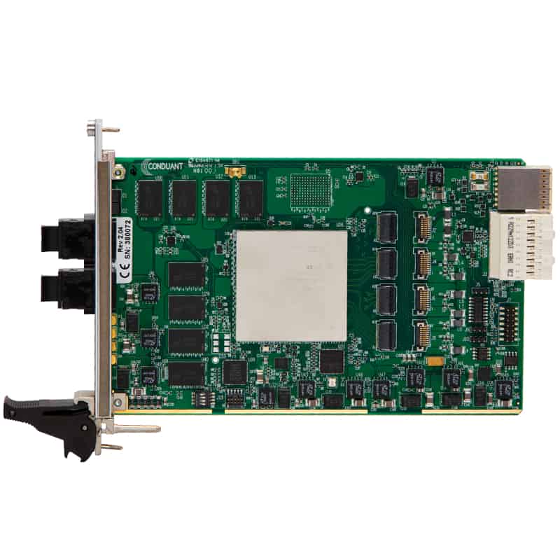
The board provides both 8GB of high-speed DDR3 SDRAM and 8MB of QDR II+ SRAM. At the center of the design is a Xilinx Kintex Ultrascale (XCKU095-FFVB1760-2-E) FPGA which interconnects all ports and other devices while supplying the additional resources that are available within the FPGA. Other models of Kintex FPGAs may be available; check with your Conduant sales representative.
With up to 48 optical fibers available, the board can be used for numerous applications that require high speed data connectivity. Each lane of optical fiber (transmit or receive) can operate independently. There are also dual Interlaken cores available in the FPGA which can be used to create dual 150 Gbps Interlaken connections (12 x 12.5 Gbps). Other optical protocols (i.e. Serial FPDP, Aurora, etc.) can also be used and a copper cabling option is available.
At power-on, the Kintex Ultrascale FPGA is quickly configured with the user program by using the SPI x4 serial flash memory device. This provides the fast wake-up required for PCI Express. The user content can be encrypted using a key that is either permanently programmed in a non-volatile manner into the FPGA (eFUSE) or can be preserved in a volatile manner so long as the on-board battery is not removed. This feature makes this product particularly attractive for applications in which protecting the FPGA intellectual property from cloning or reverse engineering is important.
The board includes a microcontroller for power management and an on-board I2C interface connecting the uC, FPGA, and optical transceivers.
For users who need more FPGA resources than are available in the XCKU095-FFVB1760-2-E, the pinout has been chosen to support migration to other, pin-compatible, Virtex/Kintex Ultrascale components. These variations can be provided by request.

