This website uses cookies so that we can provide you with the best user experience possible. Cookie information is stored in your browser and performs functions such as recognising you when you return to our website and helping our team to understand which sections of the website you find most interesting and useful.
-
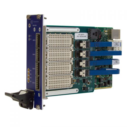
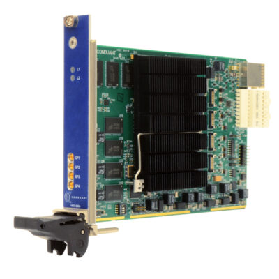
The HSS-8316-DSP FPGA board is a user programmable hardware platform with an 8-lane Gen3 PXI Express (PXIe) interface. It includes four QSFP ports (16 lanes) to support High Speed Serial (HSS) connections. The PXIe interface provides a maximum throughput of 8 GB/s while each QSFP port has 4 lanes supporting full duplex transfers at rates over 64 Gbps.
The board includes 8 GiB of DDR3 SDRAM and 8 MiB of QDR II+ SRAM. At the center of the design is an AMD Kintex Ultrascale FPGA which interconnects all ports and other devices while supplying additional resources within the FPGA. This particular FPGA contains a high count of DSP elements which uniquely suits this board for signal processing.
With the HSS lanes and 4 MMCX coaxial connections available, the board can be used for numerous applications that require high speed data connectivity with advanced DSP functionality. Each HSS lane can operate independently or in a bonded configuration if supported by the protocol being used. Popular HSS protocols that can be implemented include AMD Aurora, Interlaken, Serial FPDP, and ODI (Optical Data Interface) using optical or copper connectivity.
The FPGA is quickly loaded using the SPI x4 serial flash memory device. This provides the fast wake-up required for PCI Express. The user content can be encrypted with a key that is programmed in the FPGA in non-volatile EFUSEs or can be preserved in volatile memory so long as the on-board battery is not removed. This feature makes this product particularly attractive for applications in which protecting the FPGA intellectual property from cloning or reverse engineering is important.
To improve clocking flexibility, the board includes a Skyworks part that supports both integer and fractional divides. The provided VHDL project uses the internal I2C bus to initialize these clocks at power-up for the self test function and the user can also access the I2C bus if different frequencies are needed.
Keep in Touch
Interested in learning more about this product? Provide your contact information and someone from our team will reach out.
-

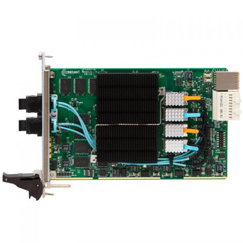
The Conduant HSS-8324 Optical FPGA board provides the user with a hardware platform that is able to sustain full-duplex high-bandwidth transfers through its 8-lane Gen3 PXI Express (PXIe) interface and its 24-lane optical interface. The PXIe interface provides a theoretical maximum throughput of 8GB/s (simultaneous in and out).
The board provides both 8GB of high-speed DDR3 SDRAM and 8MB of QDR II+ SRAM. At the center of the design is a Xilinx Kintex Ultrascale (XCKU095-FFVB1760-2-E) FPGA which interconnects all ports and other devices while supplying the additional resources that are available within the FPGA. Other models of Kintex FPGAs may be available; check with your Conduant sales representative.
With up to 48 optical fibers available, the board can be used for numerous applications that require high speed data connectivity. Each lane of optical fiber (transmit or receive) can operate independently. There are also dual Interlaken cores available in the FPGA which can be used to create dual 150 Gbps Interlaken connections (12 x 12.5 Gbps). Other optical protocols (i.e. Serial FPDP, Aurora, etc.) can also be used and a copper cabling option is available.
At power-on, the Kintex Ultrascale FPGA is quickly configured with the user program by using the SPI x4 serial flash memory device. This provides the fast wake-up required for PCI Express. The user content can be encrypted using a key that is either permanently programmed in a non-volatile manner into the FPGA (eFUSE) or can be preserved in a volatile manner so long as the on-board battery is not removed. This feature makes this product particularly attractive for applications in which protecting the FPGA intellectual property from cloning or reverse engineering is important.
The board includes a microcontroller for power management and an on-board I2C interface connecting the uC, FPGA, and optical transceivers.
For users who need more FPGA resources than are available in the XCKU095-FFVB1760-2-E, the pinout has been chosen to support migration to other, pin-compatible, Virtex/Kintex Ultrascale components. These variations can be provided by request.
Keep in Touch
Interested in learning more about this product? Provide your contact information and someone from our team will reach out.
-
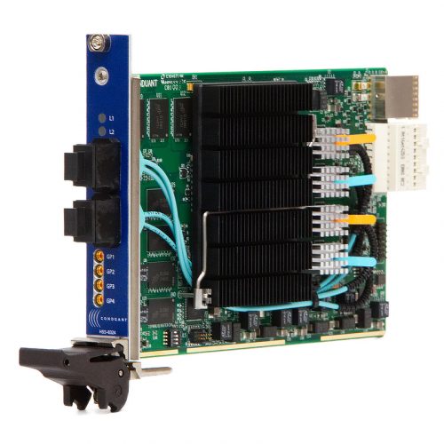
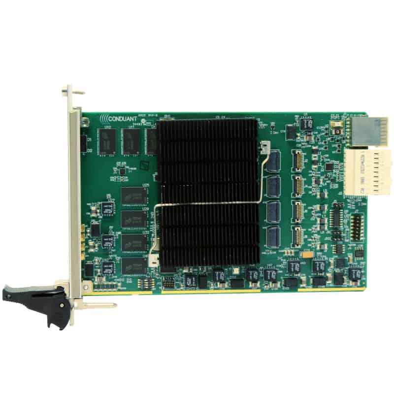
The Conduant HSS-8324 FPGA board provides a user programmable hardware platform that is able to sustain full-duplex high-bandwidth transfers through its 8-lane Gen3 PCI Express interface and its two 12-lane HSS interfaces while performing complex calculations. The PCIe interface provides a theoretical maximum throughput of 8 GBps (simultaneous in and out) while each HSS port (12 lanes up to 16 Gbps per lane) supports a full duplex transfer at theoretical rates over 190 Gbps.
The board includes both 8 GiB of high-speed DDR3 SDRAM and 8 MiB of QDR II+ SRAM. At the center of the design is an AMD (Xilinx) Kintex Ultrascale FPGA which interconnects all ports and other devices while supplying additional resources within the FPGA. This particular FPGA contains a high count of DSP elements which uniquely suits this board for signal processing.
With up to 24 HSS lanes and 4 MMCX coaxial connections available, the board can be used for numerous applications that require high speed data connectivity with advanced DSP functionality. Note that each HSS lane can operate independently or in a bonded configuration if supported by the protocol being used. Popular HSS protocols that can be implemented include but are not restricted to Aurora, Interlaken, Serial FPDP and ODI (Optical Data Interface) with optical or copper connectivity.
At power-on, the FPGA is quickly configured with the user program by the SPI x4 serial flash memory device. This provides the fast wake-up required for PCI Express. The user content can be encrypted with a key that is programmed in the FPGA in non-volatile EFUSEs or can be preserved in volatile memory so long as the on-board battery is not removed. This feature makes this product particularly attractive for applications in which protecting the FPGA intellectual property from cloning or reverse engineering is important.
To improve clocking flexibility, the board includes a Skyworks Si5341B part that supports both integer and fractional divides. While the provided VHDL project uses the internal I2C bus to initialize these clocks at power-up for the self test function, the user can access the I2C bus if different frequencies are needed.
Other models of Kintex or Virtex Ultrascale FPGAs may be available.
Keep in Touch
Interested in learning more about this product? Provide your contact information and someone from our team will reach out.
-
The Conduant HSS-8324-DSP FPGA board provides a user programmable hardware platform that is able to sustain full-duplex high-bandwidth transfers through its 8-lane Gen3 PXI Express (PXIe) interface and its two 12-lane HSS interfaces while performing complex calculations. The PXIe interface provides a theoretical maximum throughput of 8 GBps (simultaneous in and out) while each HSS port (12 lanes up to 16 Gbps per lane) supports a full duplex transfer at theoretical rates over 190 Gbps.
The board includes both 8 GiB of high-speed DDR3 SDRAM and 8 MiB of QDR II+ SRAM. At the center of the design is an AMD (Xilinx) Kintex Ultrascale FPGA which interconnects all ports and other devices while supplying additional resources within the FPGA. The FPGAs available on this board contain a high count of DSP elements which uniquely suits this board for signal processing.
With up to 24 HSS lanes and 4 MMCX coaxial connections available, the board can be used for numerous applications that require high speed data connectivity with advanced DSP functionality. Note that each HSS lane can operate independently or in a bonded configuration if supported by the protocol being used. Popular HSS protocols that can be implemented include but are not restricted to Aurora, Interlaken, Serial FPDP, and ODI (Optical Data Interface).
At power-on, the FPGA is quickly configured with the user program by the SPI x4 serial flash memory device. This provides the fast wake-up required for PCI Express. The user content can be encrypted with a key that is programmed in the FPGA in non-volatile EFUSEs or can be preserved in volatile memory so long as the on-board battery is not removed. This feature makes this product particularly attractive for applications in which protecting the FPGA intellectual property from cloning or reverse engineering is important.
To improve clocking flexibility, the board includes a Skyworks clock synthesis part that supports both integer and fractional divides. While the provided VHDL project uses the internal I2C bus to initialize these clocks at power-up for the self test function, the user can access the I2C bus if different frequencies are needed.
Keep in Touch
Interested in learning more about this product? Provide your contact information and someone from our team will reach out.
-
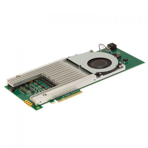
The Conduant PXIe-8300 FPGA board provides a hardware platform that is able to sustain full-duplex high-bandwidth transfers through its 8-lane Gen3 PXI Express (PXIe) interface and its 24 channel high speed serial interface. The PXIe interface provides a theoretical maximum throughput of 8GB/s (simultaneous in and out). At the center of the design is a Xilinx Kintex Ultrascale (XCKU095-FFVB1760-2-E) FPGA which interconnects all ports and other devices in addition to the resources available within the FPGA. The board provides both 8GB of high-speed DDR3 SDRAM and 8MB of QDR II+ SRAM for data storage or buffering.
With up to 24 high speed serial transceivers available, the board can be customized to include a front panel connector (optical or copper) to gain access to these channels for numerous applications that require high speed data connectivity. The high speed serial lanes are implemented on the board as connections for Samtec Firefly modules which allows numerous options for copper or optical cabling to match your requirements. Each channel (transmit/receive) can operate independently or be combined (bonded) using various protocols to achieve higher performance. The included Interlaken cores in the FPGA can be used to create dual 150 Gbps interfaces. Additional protocols such as AMD’s Aurora serial protocol can also be used to meet your connectivity requirements for high speed data transfer.
At power-on, the FPGA is quickly loaded with the user program using the SPI x4 flash memory device. This provides the fast wake-up required for PCI Express. The user content can be encrypted using a key that is either permanently programmed in a non-volatile manner into the FPGA (eFUSE) or can be preserved in a volatile manner so long as the on-board battery is not removed. This feature makes this product particularly attractive for applications in which protecting the FPGA intellectual property from cloning or reverse engineering is important.
The board includes a microcontroller (uC) for power management and an on-board I2C interface connecting the uC, FPGA, and Samtec Firefly modules (optional).
Keep in Touch
Interested in learning more about this product? Provide your contact information and someone from our team will reach out.
-
The Conduant HSS-8324 Optical FPGA board provides the user with a hardware platform that is able to sustain full-duplex high-bandwidth transfers through its 8-lane Gen3 PXI Express (PXIe) interface and its 24-lane optical interface. The PXIe interface provides a theoretical maximum throughput of 8GB/s (simultaneous in and out).
The board provides both 8GB of high-speed DDR3 SDRAM and 8MB of QDR II+ SRAM. At the center of the design is a Xilinx Kintex Ultrascale (XCKU095-FFVB1760-2-E) FPGA which interconnects all ports and other devices in addition to the resources available within the FPGA. Other Kintex Ultrascale FPGAs may be available; check with your Conduant sales representative.
With up to 48 optical fibers available, the board can be used for numerous applications that require high speed data connectivity. Each lane of optical fiber (transmit/receive) can operate independently. There are also dual Interlaken cores available in the FPGA which can be used to create dual 150 Gbps Interlaken connections (12 x 12.5 Gbps). Other optical protocols (i.e. Serial FPDP, Aurora, etc.) can also be used and a copper cabling option is available.
At power-on, the Kintex Ultrascale FPGA is quickly loaded with the user program using the SPI x4 flash memory device. This provides the fast wake-up required for PCI Express. The user content can be encrypted using a key that is either permanently programmed in a non-volatile manner into the FPGA (eFUSE) or can be preserved in a volatile manner so long as the on-board battery is not removed. This feature makes this product particularly attractive for applications in which protecting the FPGA intellectual property from cloning or reverse engineering is important.
The board includes a microcontroller for power management and an on-board I2C interface connecting the uC, FPGA, and optical transceivers.
Keep in Touch
Interested in learning more about this product? Provide your contact information and someone from our team will reach out.